

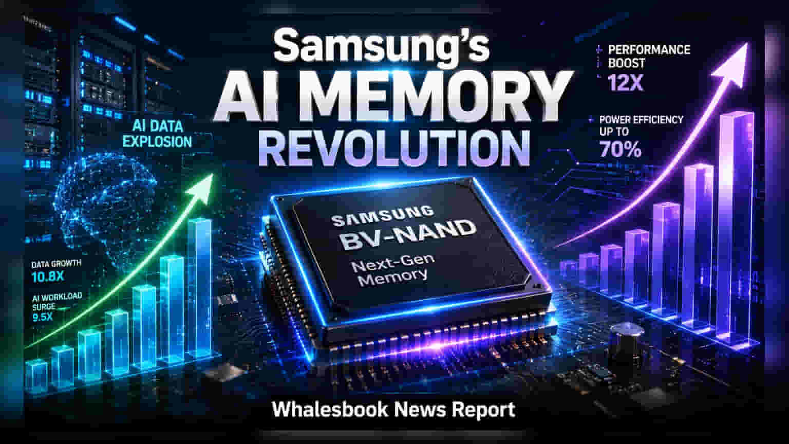
Samsung Electronics has calibrated the future of data storage by unveiling its 400-layer AI memory technology, a strategic breakthrough designed to meet the precision demands of the global artificial intelligence surge. This next-generation V10 Bonding V-NAND (BV-NAND) architecture offers a 58% increase in density, establishing a new baseline for high-performance computing. By verticalizing memory cells, Samsung is effectively removing the structural limitations of traditional hardware to fuel the next phase of machine learning evolution.
The Structural Evolution of AI Memory Technology
As AI workloads transition from training massive models to real-time inference, the demand for high-capacity NAND memory has reached a critical tipping point. Consequently, Samsung presented its V10 Bonding V-NAND prototype at the Future of Memory and Storage conference. This architecture utilizes a sophisticated wafer-bonding method that triples energy efficiency while simultaneously reducing thermal resistance by over 50%.
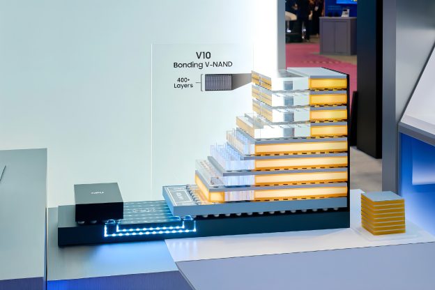
Furthermore, the integration of BV-NAND technology ensures that data-heavy applications, such as high-resolution video and complex mobile software, operate with lower latency. These structural upgrades are essential catalysts for AI systems that require rapid data access without compromising power consumption. Samsung projects that this wafer-bonding approach could eventually deliver ten times the density of current HBM5 standards.
Architecting the zHBM and zNAND-O Frontiers
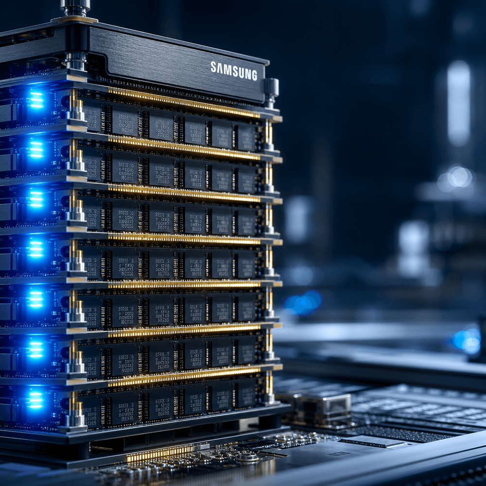
Beyond standard density increases, Samsung revealed innovative concept models for zHBM architecture and zNAND-O. In a traditional setup, high-bandwidth memory sits horizontally adjacent to AI processors. In contrast, Samsung’s zHBM design stacks memory vertically above the AI accelerators. This precision engineering reduces the physical distance data must travel, significantly increasing bandwidth and operational efficiency.
Market analysts remain highly optimistic about these developments despite fluctuating consumer smartphone demand. Samsung recently highlighted that long-term strategic agreements now represent nearly 70% of its total memory sales. This shift indicates that the global infrastructure for artificial intelligence is no longer a speculative trend but a permanent industrial baseline.
The Situation Room Analysis
The Translation
Samsung is fundamentally changing how “storage” works. Instead of just making a bigger “hard drive,” they are stacking 400 layers of memory cells directly on top of each other using “wafer-bonding.” Think of it as moving from a sprawling single-story warehouse to a high-tech skyscraper. This AI memory technology allows more data to be stored in a smaller space while moving that data to the processor much faster and using less electricity.
The Socio-Economic Impact
For the average Pakistani citizen, this innovation accelerates the localization of AI. As storage becomes denser and cheaper per gigabyte, local startups and educational institutions can run complex AI models on smaller, more affordable hardware. Students and professionals in urban centers like Karachi and Lahore will benefit from more responsive AI-driven mobile tools and cloud services, bridging the digital divide through hardware efficiency rather than just raw bandwidth.
The Forward Path
This development represents a definitive Momentum Shift. Samsung is not merely maintaining its market position; it is rewriting the physical limits of semiconductor design. By achieving a 58% density increase and tripling energy efficiency, they have provided the necessary hardware catalyst for the next decade of autonomous systems and localized AI computing.