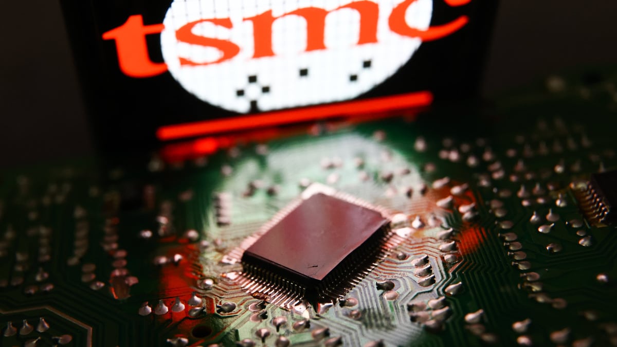
The global semiconductor landscape is undergoing a structural recalibration as TSMC develops TSMC CoPoS technology to meet the extreme demands of next-generation AI architecture. This strategic pivot from traditional wafer-based packaging to panel-level processing optimizes hardware efficiency while significantly reducing manufacturing waste. Consequently, the industry views this development as a baseline for the future of high-performance computing.
Understanding TSMC CoPoS Technology
TSMC CoPoS, or Chip-on-Panel-on-Substrate, represents a calibrated shift in how engineers assemble complex processors. Unlike conventional circular wafers, this method utilizes a rectangular panel-level packaging platform. Furthermore, the transition to rectangular substrates allows for higher chip density and a precision-engineered reduction in edge waste. TSMC plans to achieve mass production for this platform as early as 2028.
According to industry analysts, TSMC CoPoS technology integrates glass substrates sandwiched between layers of Ajinomoto Buildup Film (ABF). Specifically, glass acts as a temporary carrier during the assembly phase. This structural choice provides a more stable foundation for ultra-large packages, which are becoming the standard for modern AI accelerators.
Nvidia and the Production Roadmap
The roadmap for this technology is already becoming clear. TSMC initiated its pilot production line in early 2026, with small-volume trials expected by 2027. Consequently, industry leaders like Nvidia are already positioned as primary catalysts for adoption. Reports suggest Nvidia’s future “Feynman” AI chip will be among the first products to leverage the structural benefits of CoPoS packaging.

Strategic tool integration began in February 2026 at specialized facilities. Ultimately, TSMC aims to reach full-scale volume production between 2028 and 2029. This timeline ensures that the supply chain is prepared for the next wave of ultra-large AI packages that exceed current reticle-size limitations.
Situation Room Analysis
The Translation
In traditional manufacturing, chips are cut from circular wafers, which inherently creates unused space at the edges. TSMC CoPoS technology solves this by using rectangular panels. Imagine baking cookies: you get more cookies from a rectangular tray than a circular one because you can utilize every corner. By switching to glass substrates, TSMC also improves heat management and electrical signaling, which are critical for AI performance.
The Socio-Economic Impact
For the average Pakistani citizen, this innovation signals a gradual reduction in the cost of digital services. As AI chips become cheaper and more efficient to produce, the cost of cloud computing, AI-driven education tools, and localized data processing will decrease. For professionals and students in Pakistan, this means broader access to high-powered AI applications that were previously restricted by hardware costs.
The Forward Path
This development represents a definitive Momentum Shift. TSMC is not merely maintaining current standards; they are re-engineering the baseline of semiconductor physics. By solving the “edge waste” problem, they are providing a catalyst for cheaper, faster AI hardware. For Pakistan’s growing tech sector, following these structural shifts is essential for remaining competitive in the global digital economy.


